Indian chip startup Bharat Semi lands $24 million seed round as it eyes
Indian chip startup Bharat Semi secured $24M in seed funding to develop edge AI image sensors, landing initial defense design wins with General Atomics.
By Dillip Chowdary • Nov 15, 2026 • Source: TechCrunch
At a glance
- Funding round
- $24 million all-equity seed financing
- Target product
- Programmable AI-enabled single-chip image sensors
- Commercial delivery
- Initial volume production targeted for 2027
- Design partners
- General Atomics and Kaynes Semicon
- Company model
- Fabless semiconductor design firm
- Staff size
- Approximately 75 employees in India and the U.S.
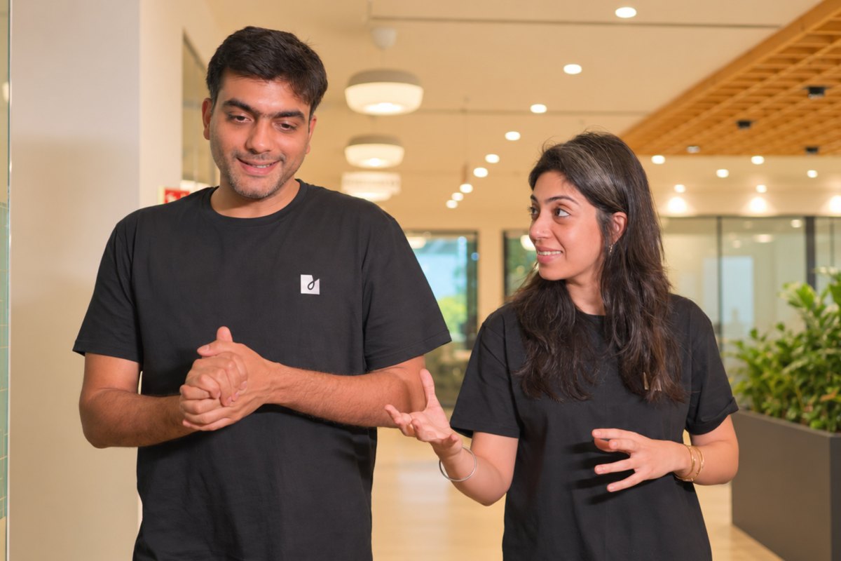
New Delhi semiconductor startup Bharat Semi has raised a $24 million seed funding round to accelerate development of its programmable artificial intelligence image sensors. According to TechCrunch's report, the nearly five-year-old pre-revenue company secured early design wins with American defense contractor General Atomics and Indian packaging firm Kaynes Semicon. The capital injection comes as India commits billions of dollars to build a domestic chip ecosystem while Western buyers diversify component sourcing beyond Chinese manufacturing hubs.
This report details Bharat Semi's single-chip sensor architecture, its commercial prototyping timelines through 2027, and its international expansion across Santa Clara and Europe. It is written for hardware engineers, procurement leaders, and semiconductor investors evaluating edge vision silicon and fabless defense suppliers. Readers will find verified specifications, executive roster details, cost reduction figures, and operational distinctions surrounding the company's separate domestic fabrication initiative.
01Seed capital and initial aerospace design wins
Bharat Semi closed its seed round as an all-equity transaction led jointly by Info Edge Group, South Park Commons, and Indus Bridge Ventures. Additional financial backing arrived from Valour Capital, consumer electronics brand Micromax, Gaingels, and several individual angel investors. Co-founder Vrinda Kapoor confirmed that the company will deploy these funds to expand its engineering roster, finalize hardware development, and introduce the sensors to international commercial buyers.
The startup secured high-profile client design wins ahead of commercial silicon availability, landing commitments from American defense contractor General Atomics and Indian semiconductor specialist Kaynes Semicon. These early agreements provide commercial validation for the startup as it attempts to break into the United States defense and industrial sectors. Company leadership highlighted that establishing overseas traction represents a critical milestone in proving that an Indian venture can build globally competitive hardware.
Note: While early customer design commitments are officially signed, the underlying sensor silicon remains under active development. Commercial volume production will not begin until 2027, meaning the pre-revenue venture must rely entirely on its balance sheet while testing engineering prototypes with partners.
02Integrated silicon architecture and cost reduction
Bharat Semi is building programmable image sensors designed to integrate visual capture, signal processing, and artificial intelligence inferencing onto a single piece of silicon. This integrated structure removes the requirement of routing raw visual data off-chip to secondary processing chips across a circuit board. According to Kapoor, integrating these discrete stages allows hardware assemblers to trim total system expenses by at least 70 percent compared to traditional assemblies.
| Architecture Component | Conventional Multi-Chip Setup | Bharat Semi Single-Chip Setup |
|---|---|---|
| Image Capture | Standalone image sensor | Integrated on-chip sensor |
| Signal Processing | Dedicated image signal processor | Integrated on-chip ISP |
| AI Inference | Separate system-on-chip or accelerator | Native on-chip AI engine |
| System Cost | Baseline hardware expense | Reduced by at least 70% |
Traditional edge camera designs typically depend on three discrete silicon packages consisting of an image sensor, an independent image signal processor, and a host system-on-chip. Consolidating those elements directly into the sensor substrate reduces interconnect bottlenecks and lowers external compute demands. Kapoor stated that the design goal is to shift hardware from basic sensors into unified sense-making solutions capable of localized evaluation.
Advertisement
Tech Pulse Daily
Get tomorrow's pulse first
Join engineers who read Tech Pulse before stand-up. Free, weekday mornings.
03Executive leadership and edge deployment targets
Vrinda Kapoor co-founded the venture in late 2021 alongside managing director Vinayak Dalmia, bringing together backgrounds in healthcare technology, management consulting at McKinsey, and private equity investment. Kapoor previously completed a fellowship at South Park Commons before establishing the company in New Delhi. Chief technology officer Boyd Fowler directs the startup's silicon architecture, having previously served as chief technology officer at commercial image sensor manufacturer OmniVision.
The company is directing its product roadmap toward four primary commercial segments: smart home consumer appliances, industrial automated facilities, security surveillance installations, and aerospace defense platforms. By embedding processing intelligence directly into the optical package, hardware designers can eliminate bulky secondary processors in constrained physical enclosures. This approach is intended to provide immediate vision analysis for automated equipment without escalating bill-of-materials costs.
Specific end-use examples cited by leadership include residential air conditioning units that identify room occupancy to modulate climate settings autonomously without external sensors. In aerospace and defense applications, unmanned drones could process visual streams in real time during flight without mounting power-hungry compute modules. These integrated packages allow peripheral edge devices to execute vision algorithms while operating under stringent battery and thermal ceilings.
04Hardware prototyping milestones and team expansion
Bharat Semi's first-generation sensors have reached the active prototyping phase, allowing internal teams to test core optical and processing functions. The engineering team is developing a second-generation sensor line featuring upgraded machine learning processing capabilities, with initial prototypes planned for mid-2027. Management projects that customer deliveries of these advanced second-generation silicon samples will commence before the end of 2027.
The startup currently employs approximately 75 people across its offices in India and the United States. Its American presence in Santa Clara includes 10 to 12 personnel handling engineering tasks alongside customer business development. Company leadership plans to expand Santa Clara staffing to approximately 20 employees by mid-2027 while initiating technical recruitment across European markets to support global design integration.
05Fabless semiconductor strategy and defense partnerships
In 2024, Bharat Semi revealed separate plans for a proposed semiconductor fabrication facility in India developed in partnership with the United States Space Force. That specialized defense manufacturing project remains under active planning as the company evaluates domestic industrial partners capable of constructing and operating the foundry. Management clarified that the capital-intensive facility venture is operated entirely apart from the core sensor product division.
Bharat Semi intends to maintain a strictly fabless operating model for its commercial image sensors, directing resources toward circuit architecture, algorithm optimization, and software development. Physical chip fabrication will be outsourced to external foundry partners rather than produced in-house. Furthermore, none of the newly closed $24 million seed capital will be allocated toward building the proposed Space Force fabrication plant.
Frequently asked questions
How much funding did Bharat Semi raise in its seed round?
Bharat Semi secured $24 million in an all-equity seed financing round led by Info Edge Group, South Park Commons, and Indus Bridge Ventures, with participation from Valour Capital, Micromax, Gaingels, and individual angel investors.
What architectural advantages do Bharat Semi image sensors offer?
The company combines optical image capture, image signal processing, and artificial intelligence execution onto a single silicon die. This integrated approach reduces overall system implementation costs by at least 70 percent compared to legacy multi-chip configurations.
When will Bharat Semi sensors enter commercial production?
First-generation sensors are currently in active prototyping, while second-generation sensors with advanced machine learning capabilities are slated to prototype by mid-2027. Bharat Semi plans to deliver second-generation units to commercial customers by late 2027.
Will the seed investment fund the proposed Space Force fabrication plant?
No, the seed capital is reserved exclusively for engineering hires and fabless sensor product development. The separate semiconductor manufacturing facility proposed in partnership with the U.S. Space Force will rely on independent domestic manufacturing partners.
Sources

Author
Dillip Chowdary
Writes Tech Bytes coverage of AI, engineering, and the tools that actually ship. Editor of Tech Pulse Daily.
Related on Tech Bytes
Advertisement